Thermal Pad Selection for Optical Transceivers Engineering Guide
Thermal Pad Selection for Optical Transceivers: An Engineering Guide to Thermal Interface Materials
1. The Thermal Challenge in High-Speed Optical Transceivers
The rapid evolution of data center architectures and 5G infrastructure is driving optical transceiver speeds from 400G toward 800G and beyond. This performance scaling comes at a significant cost: power dissipation. A single pluggable optical module now consumes between 15W and 25W, with premium 1.6T form factors exceeding 30W. At these heat flux densities, the junction temperature of the internal laser diode chip becomes a critical reliability factor. Every 10°C increase in junction temperature reduces laser lifetime by approximately 50%, while also causing wavelength drift and signal integrity degradation.
Within the thermal management strategy of an optical transceiver, the thermal pad—serving as the critical thermal interface material (TIM) between the heat-generating chip and the metal housing—plays a decisive role in overall heat path efficiency. This article provides an objective, engineering-focused analysis of thermal pad selection criteria, key performance parameters, and practical application considerations for optical transceiver designs.
2. Thermal Management Requirements: A System-Level Perspective
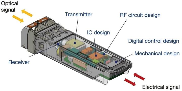
Optical transceivers present a uniquely constrained thermal environment. The internal package volume is extremely compact—typically 8–10mm in height and 18mm in width—housing multiple heat sources including the laser driver IC, transimpedance amplifier (TIA), and digital signal processor (DSP). These components exhibit high power density, with localized hot spots exceeding 85°C. However, the allowable operating temperature range is stringent: telecom-grade modules must function from -40°C to +85°C, while industrial-grade units operate from -40°C to +70°C. Exceeding these limits results in degraded optical power output, elevated bit error rates, or permanent device failure.
From a thermal path design perspective, the transceiver typically employs a metal housing as the heat spreader. Heat is transferred from the chip through the thermal interface material to the housing surface, then dissipated via system airflow or conducted to external cooling structures. Within this path, the thermal pad fills the microscopic air gaps between the chip and housing, reducing contact resistance—a critical function. Given that cumulative mechanical tolerances within the module can reach 0.2–0.5mm, and chip heights vary across the assembly, the thermal pad must exhibit sufficient compressibility to conform to non-planar surfaces.
3. Key Technical Parameters for Thermal Pad Selection
For optical transceiver applications, the following parameters should be prioritized during thermal pad selection:
3.1 Thermal Conductivity (W/m·K)
This is the primary metric characterizing a pad's heat transfer capability. For optical transceivers, thermal conductivity typically ranges from 3 to 8 W/m·K. Pads with excessively high conductivity often exhibit increased hardness, compromising conformability; conversely, insufficient conductivity fails to meet heat dissipation requirements. Critically, thermal conductivity should not be evaluated in isolation—total thermal resistance, including contact resistance, must be assessed holistically.
3.2 Thermal Impedance (°C·cm²/W)
Thermal impedance reflects the pad's actual heat transfer performance under specific applied pressure, incorporating both bulk material resistance and contact resistance. For optical transceiver applications, a thermal impedance below 1.0°C·cm²/W is recommended to maintain acceptable temperature rise between the chip and housing.
3.3 Compressive Stress and Deflection Rate
Given the confined internal space of optical modules, installation pressure is limited. The pad must achieve 15%–30% compression at relatively low applied pressures (typically 10–50 psi) to adequately fill gaps. Additionally, the pad should maintain a low compression set rate (recommended below 5%) under prolonged compression to ensure long-term reliability.
3.4 Thickness and Tolerance Control
Common pad thicknesses in optical transceivers range from 0.5mm to 2.0mm, with thickness tolerance controlled within ±0.1mm. Excessive thickness increases thermal resistance; insufficient thickness fails to fill gaps. Furthermore, thickness uniformity significantly impacts contact resistance consistency across the interface.
3.5 Temperature Resistance and Reliability
Optical transceivers operate across a wide temperature range. The pad must maintain stable performance from -40°C to +125°C without oil bleeding, hardening, or degradation. Additionally, the pad must pass 85°C/85% RH (double-85) high-temperature/high-humidity testing and 1,000-hour high-temperature aging tests.
4. Application Scenarios and Engineering Solutions
In practical optical transceiver designs, thermal pads are deployed in several critical locations:
4.1 DSP Chip to Housing Interface
The DSP is the highest-power component in the module, dissipating 8–15W. The heat path is: chip → thermal pad → metal housing → external environment. For this location, a thermal pad with 5–8 W/m·K conductivity and 1.0–1.5mm thickness is recommended, ensuring adequate conformability under limited installation pressure.
4.2 Laser Driver IC to Housing Interface
Laser diodes are extremely temperature-sensitive; temperature fluctuations directly impact output optical power stability. For this location, a thermal pad with 3–5 W/m·K conductivity and 0.5–1.0mm ultra-thin construction is recommended to minimize thermal resistance while accommodating confined space constraints.
4.3 TIA to Housing Interface
The TIA is sensitive to electromagnetic interference. Beyond heat dissipation, the pad's electrical insulation properties must be considered. A thermally conductive but electrically insulating pad with volume resistivity exceeding 10¹³ Ω·cm is recommended for this position.
Engineers must also consider pad die-cut precision and assembly processes. The compact internal space of optical transceivers means dimensional deviations could cause assembly interference or incomplete coverage. Precision die-cutting with dimensional tolerance controlled within ±0.2mm is recommended, with careful alignment between pad center and heat source during placement.
5. Recommended Solution: iTousen Thermal Pad Series
iTousen High-Performance Thermal Pads for Optical Transceivers
Addressing the stringent thermal management requirements of optical transceivers, Shenzhen iTousen Technology Co., Ltd. (iTousen) offers a series of high-performance thermal pad products specifically engineered for optical transceivers, 5G communication equipment, and other compact electronic devices. Key technical advantages include:
- High Thermal Conductivity: Multiple grades covering 3.0–8.0 W/m·K to accommodate varying chip power dissipation requirements
- Ultra-Low Thermal Impedance: As low as 0.35°C·cm²/W at 50 psi applied pressure, effectively reducing chip-to-housing temperature rise
- Superior Conformability: Achieves over 20% compression at 20 psi low pressure, perfectly adapting to non-planar surfaces within optical transceivers
- High Reliability: Passes double-85 testing and -40°C to +125°C thermal shock testing with stable long-term performance
- Precise Thickness Control: Range of 0.3mm–3.0mm with tolerance controlled within ±0.1mm, meeting precision assembly requirements
- Excellent Electrical Insulation: Volume resistivity exceeding 10¹³ Ω·cm with dielectric breakdown voltage greater than 6KV/mm, ensuring electrical safety
This product series has been widely deployed in 100G/400G/800G optical transceivers, optical transceivers, and active optical cables, effectively resolving thermal bottlenecks and enhancing long-term product reliability.
6. Conclusion
Optical transceiver thermal design is a systems engineering challenge. As the critical thermal interface material, thermal pad selection requires comprehensive evaluation of thermal conductivity, thermal impedance, compressive performance, thickness tolerance, and long-term reliability. Engineers should base their selection on actual application scenarios, combining thermal simulation analysis with empirical validation to identify the optimal thermal pad solution. The iTousen thermal pad series offers reliable material assurance for optical transceiver thermal management, supporting customers in maintaining competitive advantage in the high-speed optical communications market.
Silicone Thermal Pads for Automotive Electronics Cooling
Related Article