Silicone Thermal Pad Selection for PV Inverter Thermal Management
Thermal Interface Design for PV Inverters: How Silicone Thermal Pads Protect Power Stages
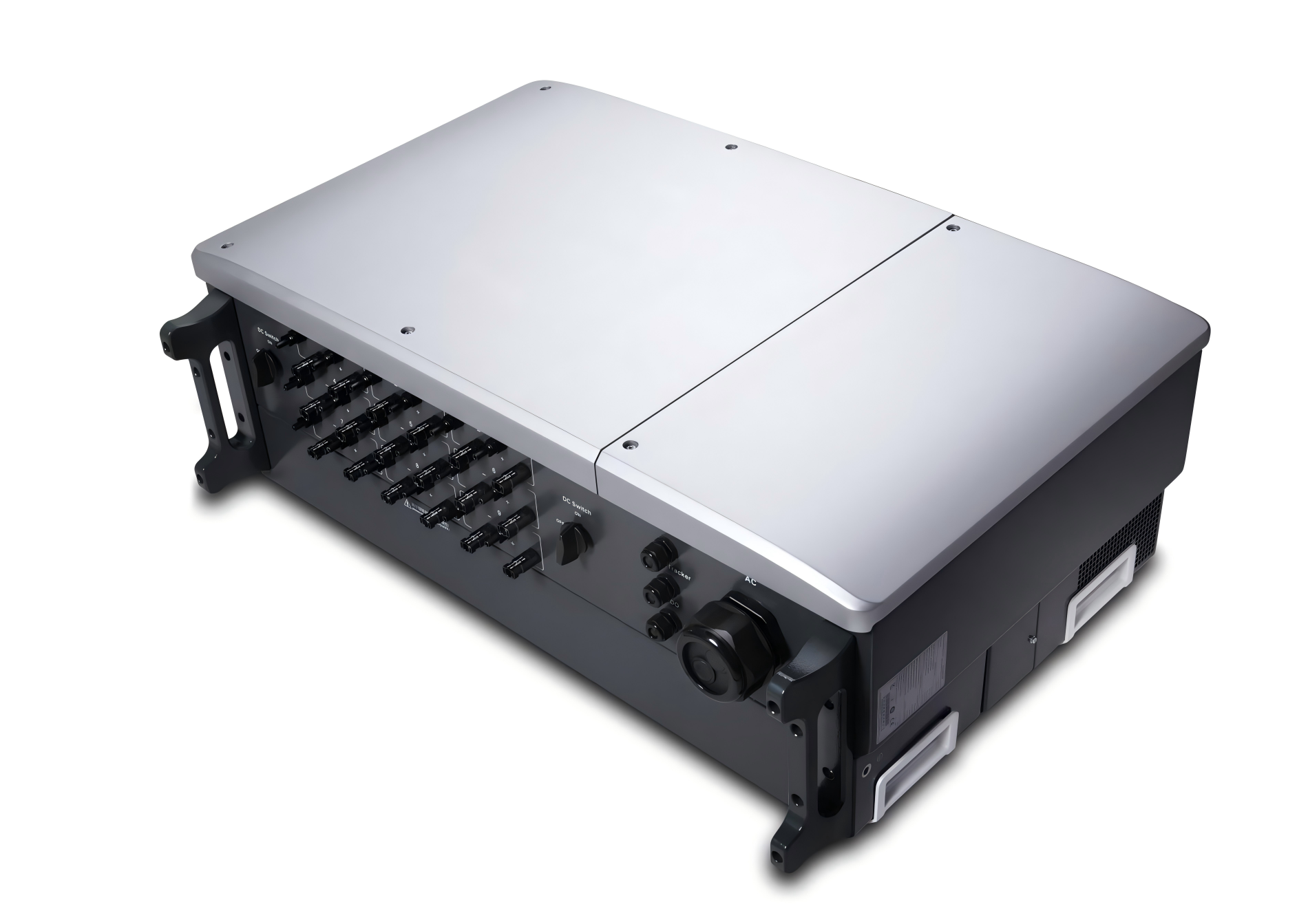
A grid-tied inverter is, thermally, a controlled experiment that must run for twenty-five years. Conversion losses of 1.5–3 % of rated output leave the IGBT or SiC stage, the DC-link capacitor bank and the output choke as the dominant heat sources, while the enclosure is often sealed to IP65 and installed where noon ambient reaches 55–60 °C. Every watt that cannot leave through the heatsink raises junction temperature, accelerates wire-bond fatigue and forces the firmware to derate exactly when irradiance peaks. In most outdoor designs the decisive part is not the heatsink but the thin layer between module and heatsink — the thermal interface material. When that layer is a silicone thermal pad, its thickness, softness and long-term stability set the derating threshold.
Why the interface, not the heatsink, is usually the bottleneck
A 50 kW string inverter may use an extruded heatsink rated 0.10–0.25 K/W. Across a 100 cm² module footprint, a 1.0 mm gap filled with a 3 W/m·K pad adds about 0.033 K/W, while a 1.5 mm gap with a 1.5 W/m·K silicone thermal pad adds roughly 0.10 K/W — the same order as the entire heatsink. Because these resistances sit in series with the junction-to-case and case-to-ambient paths, 0.05 K/W at 60 W of module loss becomes 3 °C of extra junction temperature, often the difference between a 125 °C margin and a derating event. PV inverter thermal management is settled at the drawing board, in the tolerance stack-up of the gap.
Where the heat is actually generated
Loss distribution is fairly stable across power classes, which explains why one pad grade rarely fits the whole chassis.
| Heat source | Share of loss | Limiting temperature | Typical gap | Decisive property |
|---|---|---|---|---|
| IGBT / SiC module to heatsink | 50–60 % | 125–175 °C junction | 0.2–1.0 mm | Conductivity at moderate pressure |
| DC-link film capacitors | 10–15 % | 85–105 °C case | 0.5–2.0 mm | Softness, gap filling |
| Output choke, boost inductor | 15–20 % | 105–125 °C winding | 1.0–3.0 mm | Thick forming, low oil bleed |
| Busbars, terminal blocks | 5–10 % | 90–105 °C | 0.3–1.0 mm | Dielectric strength |
| Auxiliary supply, control board | 3–5 % | 85–95 °C | 0.3–0.8 mm | Low modulus, reworkability |
Gap tolerance: the number most often specified wrong
Module flatness contributes 0.05 mm, a 200 mm extruded profile 0.10 mm, mounting bosses and weld distortion another 0.10–0.15 mm, plating and paint a further layer. The nominal 0.50 mm gap on the drawing becomes 0.30–0.90 mm on the line. A 0.50 mm pad in a 0.90 mm cavity leaves an air layer costing more resistance than the pad saves; a 0.90 mm pad in a 0.30 mm cavity over-compresses the material, lifts the module off its plane and loads solder joints.
The working rule is pad thickness at 0.85–0.90 of the maximum gap, so the loosest assembly still sees 10 % compression and the tightest stays under 30 %. Thermal grease wins only when the gap is below 0.1 mm and the surfaces are machined. For cast or extruded housings, for field-serviceable modules and for any design exposed to vibration and repeated thermal cycling, a silicone thermal pad avoids pump-out, migration and the contamination grease brings into a sealed enclosure.
Parameters that actually predict performance
- Impedance, not headline conductivity. Bulk conductivity is measured on a void-free sample; the inverter sees impedance at the real clamp pressure, often 10–20 psi on a plastic module housing. Request impedance at 10, 20 and 30 psi.
- Compressibility and hardness. A 40 Shore 00 pad conforms at low pressure and protects ceramic substrates; a 60 Shore 00 grade resists extrusion in thin, high-pressure joints.
- Dielectric strength. The pad insulates a live module from a grounded heatsink and must survive the 3–5 kV hipot test at the specified thickness, after ageing.
- Flame rating. UL94 V-0 is effectively mandatory inside an inverter enclosure, with RoHS, halogen-free and REACH compliance for Europe.
- Oil bleed and siloxane volatility. Low-molecular siloxane fogs indicators and contaminates relay contacts; specify bleed below 1 % after 24 h at 150 °C.
- Long-term stability. Properties must hold from −50 °C to 200 °C and survive 1,000 h at 150 °C without hardening beyond the compression-set limit.
Matching the grade to the position in the chassis
The SF Series from TOUSEN covers 1.5–15.0 W/m·K in 0.3–10.0 mm sections, allowing one approved material family from the power module down to the auxiliary board.
| Grade | W/m·K | Impedance, 1 mm @ 30 psi (°C·in²/W) | Thickness | Typical location |
|---|---|---|---|---|
| SF100 | 1.5 | 0.90 | 0.3–10.0 mm | Control board, auxiliaries |
| SF400 | 2.5 | 0.50 | 0.3–10.0 mm | DC-link capacitors, EMI filter |
| SF500 | 3.0 | 0.45 | 0.3–10.0 mm | Choke clamping, thick gaps |
| SF600G | 6.0 | 0.30 | 0.5–5.0 mm | IGBT module to heatsink |
| SF800 | 8.0 | 0.22 | 0.5–5.0 mm | High-power modules, 0.5–1.0 mm |
| SF1200 | 12.0 | 0.15 | 0.8–5.0 mm | SiC stages, compact designs |
Power module to heatsink
For a 0.5–1.0 mm gap at 20–30 psi, a 5–8 W/m·K silicone thermal pad at 40 Shore 00 gives the lowest total resistance without point loads on the substrate. Above 8 W/m·K the gain per step flattens, and the extra cost is hard to justify unless the die runs above 150 °C.
Capacitors and magnetics
Film capacitors and chokes are large, low-pressure interfaces where 2.5–3.0 W/m·K material at 0.3–1.0 mm beats a thin, hard pad: it fills the curvature of a wound element and a cast housing without stressing the leads. Sections of 2–3 mm are common on choke clamps, where the pad also damps vibration, and PV inverter thermal management in the magnetic compartment is usually limited by the housing rather than by the winding.
1500 V central inverters
Multi-module architectures place four to eight parallel bridges on one heatsink, so current sharing depends on temperature symmetry. Uniform compressed thickness across all positions matters more than one grade step of conductivity; die-cut parts with a 0.2 mm edge margin and carrier film guarantee the same installed thickness on every module.
Qualification tests to write into the specification
Measure steady-state impedance to ASTM D5470 at three pressures and two thicknesses rather than reading a marketing chart. Run compression set to ASTM D395 method B after 22 h at 70 °C, because the pad is installed once and compressed for its whole service life. Cycle from −40 °C to 105 °C for 500 cycles and hold damp heat at 85 °C / 85 % RH for 1,000 h to expose the delamination and hardening that appear after the second summer. Verify dielectric strength after ageing at the thinnest point of the die-cut part, and measure oil bleed gravimetrically at 150 °C. The thermal interface material is the only layer of the stack-up that cannot be inspected once the module is bolted down, so sample-based testing carries the whole reliability risk.
Assembly and field-service notes
- Store at 10–30 °C, away from UV and ozone; shelf life is 24 months and expires faster on an open shelf.
- Never reuse a pad after disassembly — compression set is permanent and the material has lost both thickness and wetting.
- Tighten module screws in a cross pattern in two stages and verify compression on the first unit of each batch.
- Handle silicone thermal pads with clean gloves; dust or grease on the surface adds contact resistance that no clamp pressure removes.
- Standard sheets are 200 × 300 mm; die-cut parts at 0.1 mm tolerance remove the error hand-cut pieces introduce.
Conclusion
PV inverter thermal management is a chain of series resistances, and the interface is the link easiest to get wrong and cheapest to correct. Specify the gap from measured data, the impedance at the pressure the hardware applies, and the dielectric and flame performance the certification body will test. A correctly sized silicone thermal pad then behaves as a mechanical component as much as a thermal one: it absorbs tolerance, damps vibration, insulates the module and keeps conducting for twenty-five years.
For the full parameter set, thickness options and die-cut capability of the thermal interface material described above, see the SF Series silicone thermal pad specification page, where samples can be requested for gap and pressure validation on your own hardware.
Why Silicone Thermal Pads Beat Grease for Automotive Electronics
Related Article