Thermally Conductive Paste Selection for Peltier Cooling Interfaces
Thermally Conductive Paste in Peltier Cooling: Why Bond Line Thickness Decides the Result
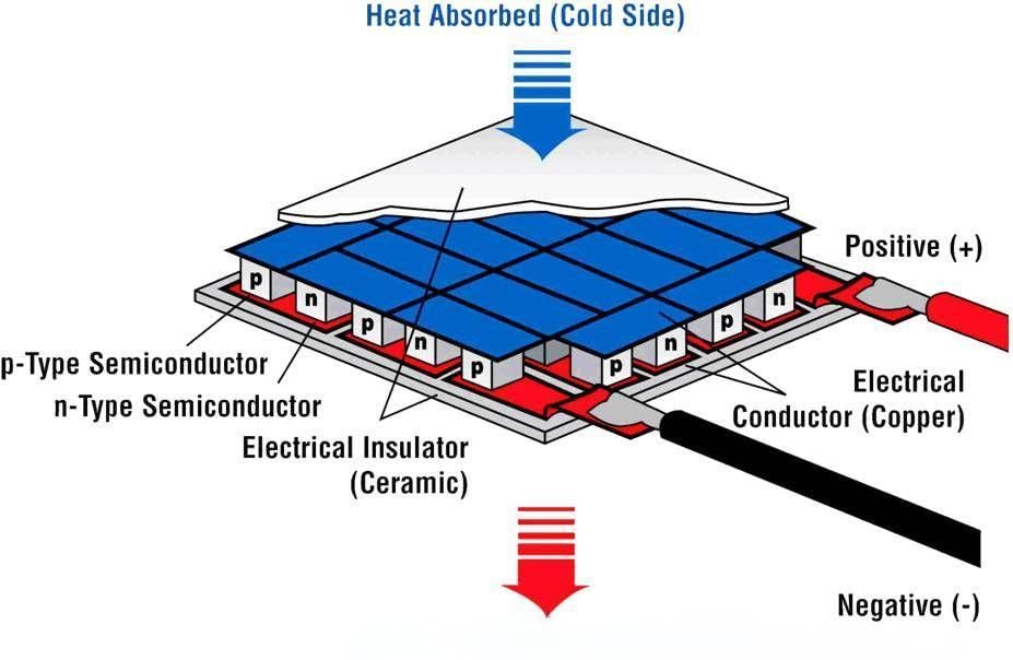
A thermoelectric cooler is the one place in electronics where 10 W/cm2 of heat flux is routine. A 40 x 40 mm module pumping 60 W draws roughly 100 W, so 160 W must cross a 16 cm2 ceramic face into a cold plate. At that flux the interface is not a second-order correction: a 0.5 mm filler costing 6 K is acceptable on a power module and unacceptable here, because the module's usable temperature difference is the currency being spent. This is where thermoelectric cooler thermal management stops being a heatsink question: a thermally conductive paste wins on physics rather than convenience, and it has to be specified by bond line thickness rather than by the conductivity printed on the jar.
Why a paste fits a Peltier stack and a pad often does not
Two conditions decide whether the thermal interface material should be grease or a solid pad, and a thermoelectric assembly usually satisfies both of them on the hot side. The ceramic face is lapped flat, so there is no gap to fill, and the clamp pressure is low but the flux is high, so every micron of interface thickness is expensive.
| Condition | Thermally conductive paste | Silicone pad |
|---|---|---|
| Interface flatness better than 0.05 mm | Preferred, BLT 20–50 µm | Works, but adds 0.3–1.0 mm |
| Tolerance stack above 0.2 mm | Cannot bridge the gap | Preferred |
| Insulation required between live and grounded parts | Not a dielectric barrier | Preferred, dielectric strength is a rated property |
| Frequent rework or field service | Preferred, no residue layer to peel | One-time use only |
| Vertical or inverted mounting | Needs low-slump thixotropic grade | Preferred, no migration |
| Optics sharing the enclosure | Requires low siloxane volatility | Requires low bleed, same check |
The number that matters: impedance times flux
The temperature rise across an interface is simply its thermal impedance multiplied by the heat flux. At 10 W/cm2 a paste measuring 0.03 °C·cm2/W adds 0.3 K, one measuring 0.05 °C·cm2/W adds 0.5 K, and a 0.201 °C·cm2/W grade adds 2.0 K. Put those figures next to a 0.5 mm pad at 8 W/m·K, which contributes roughly 6 K, and the choice of thermal interface material is settled by arithmetic rather than preference.
| Measured impedance @ 30 psi (°C·cm2/W) | Rise at 8 W/cm2 | Rise at 10 W/cm2 | Typical use |
|---|---|---|---|
| 0.201 | 1.6 K | 2.0 K | Low-power module, LED plate, secondary heat path |
| 0.080 | 0.6 K | 0.8 K | General purpose hot side |
| 0.050 | 0.4 K | 0.5 K | Standard 40 x 40 mm module |
| 0.030 | 0.2 K | 0.3 K | High flux, thin printed layer |
Where the interface sits in a real cooling stack
In thermoelectric cooler thermal management three interfaces are treated differently. The cold side carries only the pumped load and is usually a small plate or a bonded sensor; the hot side carries pumped load plus input power and must be printed thin; the driver board is a conventional low-flux problem where the choice barely matters.
| Interface | Flux | Method | Reason |
|---|---|---|---|
| Object or sensor to cold plate | 2–6 W/cm2 | Thin paste, 30–50 µm | Irregular surface, low pressure, reworkable |
| Cold plate to TEC cold ceramic | 2–6 W/cm2 | Screen-printed paste | Flat ceramic, minimal BLT, no grease starvation |
| TEC hot ceramic to heatsink | 8–12 W/cm2 | Stencil paste, 20–40 µm | Highest flux in the product, BLT dominates |
| TEC to cast or plastic frame | < 1 W/cm2 | Pad, not paste | Gap and tolerance, not conduction |
| Driver board to chassis | 0.5–2 W/cm2 | Paste or pad | Convenience and cost decide |
The five failure modes of grease in thermoelectric hardware
Pump-out. Power cycling pushes the paste outward from the centre of the interface as the parts move differentially. A non-curing thixotropic compound with low slump slows it, but the only reliable check is 1,000 cycles followed by an impedance re-measurement on the assembled stack.
Dry-out and oil separation. Oil migrating out of the filler network leaves a dry, high-resistance film at the very centre of the joint. Specify oil separation after 24 h at 150 °C rather than relying on the word "stable".
Over-application. A thick printed layer protects nothing and costs kelvin. Coverage of 80–90 percent with a 0.1 mm stencil is the normal target; a bead squeezed out at the edges during clamping is a sign of excess, not of quality.
Contamination. Low-molecular siloxane from any silicone-based paste can fog a laser window or a sensor cover inside the same enclosure, so volatility matters wherever optics are present.
False expectations about insulation. Paste is a thermal interface material, not a dielectric barrier. A 30 µm film will not carry a safety-rated withstand voltage, and any design that needs isolation between a live module and a grounded cold plate should use an insulating pad and accept its extra thickness.
Selecting the grade and printing it correctly
The TSAD Series from TOUSEN is a solvent-free, non-curing, thixotropic paste in gray, spanning 1.2–6.5 W/m·K with measured impedance from 0.201 down to 0.03 °C·cm2/W at 30 psi, specific gravity 2.5–2.9 g/cm3 and a 12-month shelf life. In a Peltier stack, thermally conductive paste is selected by the flux it has to carry and the bond line the process can hold, not by the highest conductivity grade available.
| Grade | W/m·K | Impedance @ 30 psi (°C·cm2/W) | Density (g/cm3) | Typical position |
|---|---|---|---|---|
| TSAD60 | 1.2 | 0.201 | 2.5 | Driver board, bracket, secondary path |
| TSAD66 | 3.5 | 0.080 | 2.7 | Cold-side plate, sensor mount |
| TSAD66-P | 4.0 | 0.070 | 2.6 | Cold side with rough plate finish |
| TSAD83 PLUS | 5.2 | 0.050 | 2.6 | Standard hot side of a 40 W module |
| TSAD88 PLUS | 5.2 | 0.030 | 2.9 | Thin-printed hot side, high filler loading |
| TSAD90 | 6.5 | 0.030 | 2.7 | Hot side above 10 W/cm2 |
| TSAD100 | 6.5 | 0.030 | 2.8 | Highest flux, minimum BLT target |
Stencil and coverage
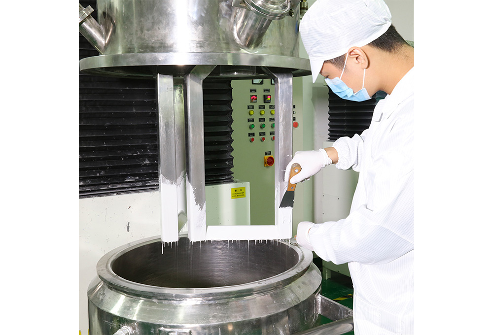
Print with a 0.1 mm stainless stencil in a dot or grid pattern at 80–90 percent coverage: dots let paste flow under pressure without trapping air, while a solid print pumps air in from the edges. A 0.2 mm stencil on a 40 x 40 mm face deposits about twice the required mass and adds several tenths of a kelvin.
Verifying the bond line
Weigh a printed coupon before and after assembly for mass per area, then divide by specific gravity: 1 mg/cm2 at 2.7 g/cm3 is about 3.7 µm of bond line. The check costs a laboratory balance and catches stencil wear long before a thermal test does.
When a pad is still the right answer
Where the housing is cast, where the gap moves with tolerance, or where dielectric isolation is a safety function, a silicone pad is the correct component and a thermally conductive paste should not be forced into that position; field service alone is not a reason to prefer paste.
Qualification plan for a printed interface
Measure the impedance of the thermal interface material to ASTM D5470 at 10, 20 and 30 psi, since the quoted 30 psi value is rarely the pressure a low-clamp Peltier stack applies. Repeat after 1,000 power cycles and after 1,000 h at 85 °C / 85 % RH on the assembled module, inspecting coverage through a cross-section of a sacrificed unit. Check oil separation gravimetrically at 150 °C, and outgassing wherever optics or sensors share the enclosure. For products that must pass a dielectric test, confirm the isolation is provided by a pad rather than by the thermally conductive paste film. Shelf life is 12 months, so paste left from a previous build should be re-qualified rather than reused silently.
Assembly and service notes
- Clean both faces with isopropyl alcohol and let them dry; a fingerprint is a measurable resistance.
- Store the jar closed at room temperature, away from open flame; the compound is non-hazardous but not indefinitely stable.
- Never re-spread paste that has already been compressed: the filler network of the thermal interface material is disturbed and the second print carries air.
- On service, remove the old film completely with a plastic scraper and solvent; a mixed old and new layer reads worse than a fresh single layer.
- Tighten in a cross pattern in two passes and verify the joint on the first unit of each lot.
Conclusion
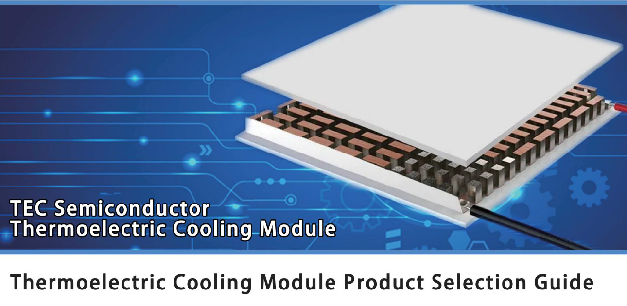
Thermoelectric cooler thermal management fails at the interface because the flux is high and the budget is small, and a thermally conductive paste is the tool that fits a flat ceramic face and a low clamp pressure. Specify it by measured impedance and by the bond line the process can hold, verify that bond line by mass rather than by eye, and reserve pads for positions where gap tolerance or dielectric isolation sets the requirement. Between a printed 30 µm layer and a generous 100 µm one sits several kelvin, which is several percent of the specified cooling capacity.
Full impedance data, conductivity grades and packaging options for the thermally conductive paste described here are listed on the TSAD Series thermal paste product page, where samples can be requested for print trials on your own cold plate.
Phase Change Thermal Pad for Advanced Electronics Cooling
Related Article