
Thermal Pad Solutions for Imaging Device Thermal Management
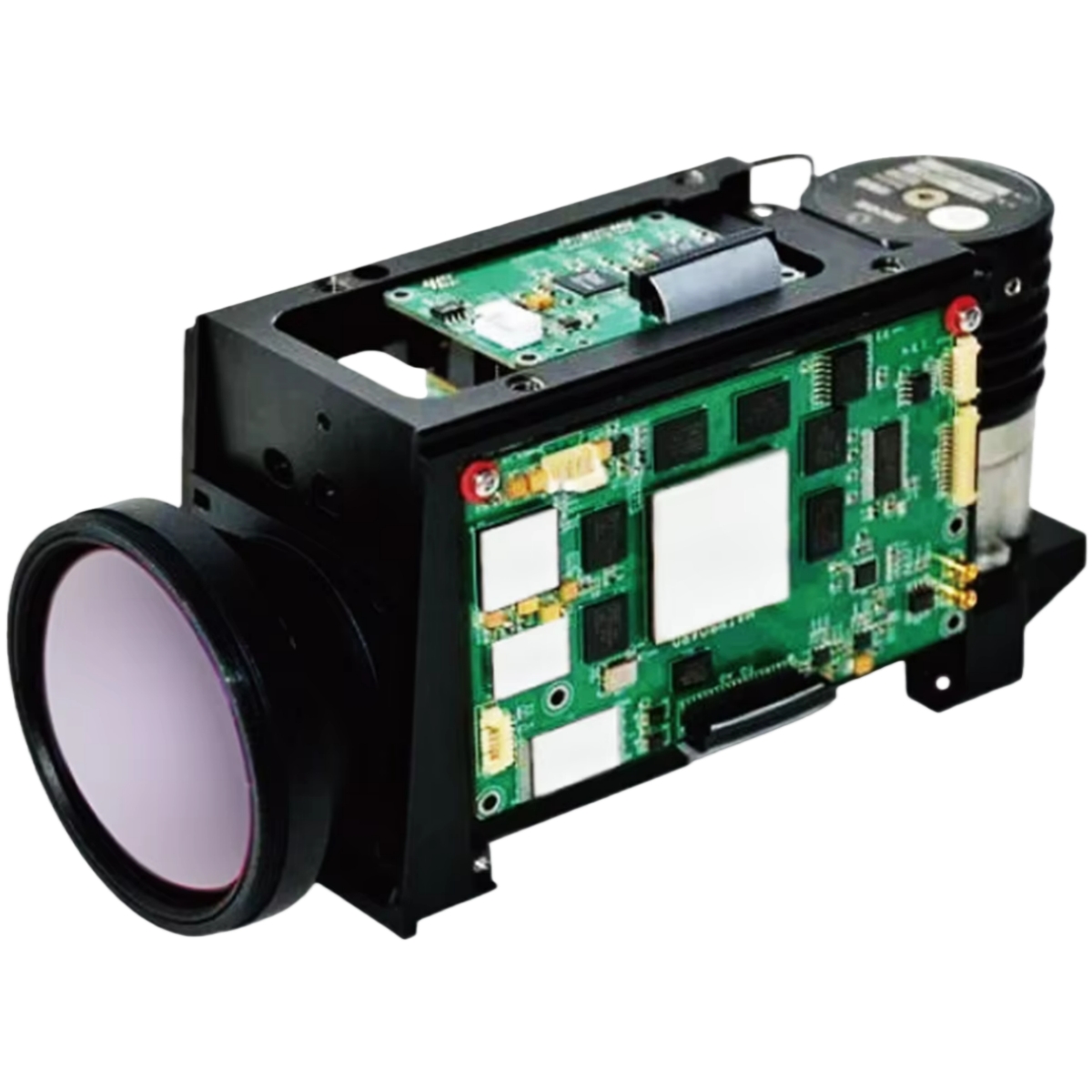
Thermal Pad Solutions for Imaging Devices: An Engineering Perspective
As imaging systems continue to evolve toward higher resolution, compact architectures, and increased processing power, thermal management has become a critical factor affecting both system reliability and image quality. From an engineering standpoint, managing heat efficiently within constrained mechanical designs is no longer optional—it is fundamental.
Among various thermal interface materials (TIMs), the thermal pad has emerged as a highly reliable and scalable solution for modern imaging devices, including industrial cameras, infrared modules, and AI-powered vision systems.
Thermal Challenges in Modern Imaging Systems
Key heat-generating components in imaging devices typically include CMOS/CCD sensors, image signal processors (ISP), FPGA or AI chips, and power management units. During high-speed data processing, these components generate localized heat that can significantly impact system performance.
If not properly managed, excessive thermal buildup can lead to increased image noise, reduced processing efficiency, and long-term reliability concerns. For precision imaging applications, even minor thermal fluctuations can degrade output quality.
The Role of Thermal Pad in Heat Dissipation
A thermal pad is designed to bridge microscopic air gaps between heat sources and heat sinks, significantly improving thermal transfer efficiency. Due to its conformability and stable material properties, it is widely used in passive cooling architectures.
1. Interface Gap Filling
Surface imperfections between chips and heat spreaders create air pockets, which act as thermal insulators. A properly selected thermal pad eliminates these gaps, reducing interface thermal resistance and ensuring consistent heat flow.
2. Passive Thermal Path Construction
In fanless imaging systems, thermal pad materials are commonly integrated with aluminum heat sinks, metal housings, or graphite sheets. This configuration enables efficient heat conduction from the source to a larger dissipation area, supporting stable operation without active cooling.
3. Electrical Insulation and Mechanical Stability
Compared to thermal grease, a thermal pad provides electrical insulation, structural integrity, and ease of assembly. It does not pump out or migrate over time, making it particularly suitable for compact and high-density designs.
Key Engineering Parameters for Thermal Pad Selection
Thermal Conductivity
Typical values range from 1 to 10 W/m·K. High-performance imaging processors generally require thermal pad materials with conductivity above 5 W/m·K to maintain optimal junction temperatures.
Thickness Optimization
Thickness must be carefully matched to mechanical tolerances. Excess thickness increases thermal resistance, while insufficient thickness may result in incomplete surface contact. Common ranges fall between 0.5 mm and 3 mm.
Compressibility and Elastic Recovery
A high-quality thermal pad should exhibit excellent compressibility to accommodate surface irregularities, along with strong elastic recovery to maintain long-term performance stability.
Operating Temperature Range
Industrial imaging devices often require materials capable of operating between -40°C and 125°C or higher, ensuring reliability under extreme conditions.
Typical Application Areas in Imaging Devices
From a system design perspective, thermal pad materials are strategically placed in the following locations:
- Between image sensors and heat sinks to minimize thermal noise
- Between ISP chips and metal enclosures for efficient heat spreading
- On power modules to prevent localized hotspots
- Across multi-chip layouts to achieve thermal balance
Proper placement of thermal pad materials not only enhances thermal efficiency but also contributes to uniform temperature distribution across the device.
Why Silicone-Free Thermal Pad Solutions Matter
In high-end imaging applications, traditional silicone-based materials may introduce risks such as outgassing, oil bleed, and contamination of sensitive optical components. These issues can compromise long-term system stability.
To address these challenges, silicone-free thermal pad solutions are increasingly adopted in precision imaging systems.
Learn more about advanced solutions here:
Silicone-Free Thermal Pads

Key Advantages
- No silicone contamination, ideal for optical environments
- Stable thermal conductivity for high-power components
- Excellent long-term reliability without drying or bleeding
- Customizable thickness and material properties
Engineering Case Insight
In a recent industrial camera project, an ISP module with approximately 8W power dissipation was operating in a 60°C ambient environment. By implementing a high-performance thermal pad with 6 W/m·K conductivity:
- Chip temperature was reduced by approximately 12°C
- Image noise levels were significantly improved
- System stability increased by over 30% during extended operation
This demonstrates that selecting the right thermal pad is not just a thermal decision—it directly impacts imaging performance and system reliability.
Conclusion
From an engineering perspective, the thermal pad plays a critical role in bridging heat sources and dissipation structures within imaging devices. Its function extends beyond simple heat transfer—it is an essential component in ensuring performance stability, image clarity, and product longevity.
As imaging technologies continue to advance, demand for high-performance, contamination-free, and customizable thermal pad solutions will only increase. Engineers and designers must therefore prioritize material selection as part of a holistic thermal management strategy.
High Performance Thermal Pad for Reliable Heat Management
High Performance Thermal Pad Solutions for EV Charging Systems
Related Article